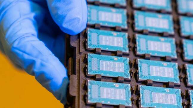
Intel thinks glass substrates are a clear winner in multi-die packaging
Don't get too excited, tech won't be ready until the end of the decade
Intel's latest gambit to keep Moore's Law on life support involves ditching organic substrates — the intermediary through which data and power flows on its way in and out of a compute die — for glass ones.
In a blog post Monday, the x86 giant revealed its working to commercial glass substrates, which it believes are key to achieving higher density, higher performance chips for applications like artificial intelligence and machine learning.
"Today's computers are increasingly using multiple chips on one substrate. As these substrates take on more silicon, our current organic substrates — mostly plastic — can warp. Glass is more rigid and can handle more chips on a package," Intel's Rob Kelton explained in a brief video. "Glass enables 50 percent more die content on the same package size than organic substrates."
The announcement comes as the chipmaker plays up its advanced packaging technologies, including embedded multi-die interconnect bridge (EMIB) and Foveros, which are used in 2D and 3D packaging of chiplets. But while the technologies deal with how various chiplets are interfaced and powered, Intel's latest developments are based on the medium on which those dies are integrated.
The idea here is rather straightforward, according to Gartner analyst Gaurav Gupta, and involves replacing the PCB core found in organic substrates with a glass one. This, he tells The Register, presents a number of benefits including superior optical and mechanical properties. For instance, glass has a thermal expansion rate closer to that of silicon, which, as we understand it, should help to mitigate the potential for warping or shrinkage.
The ability to tolerate higher temperatures is notable as Intel sees the first applications of glass substrates being in large datacenter, AI, and graphics applications, where the density of chiplets — which often operate at within wildly different temperature envelopes — might be packaged together. As we've previously covered, the thermal stress associated with these kinds of multi-die packages are one of the problems Intel is trying to address through new testing and validation regimes.
The US chip giant also contends glass' properties allow for greater interconnect densities. It estimates that glass substrates could enable a tenfold increase in interconnect densities. In other words, glass substrates should allow more data to flow in and out of the processor faster. One of the ways Intel expects to do this is by integrated optical interconnects, directly into the substrate.
The use of silicon photonics is a technology Intel has been playing with for years now. Most recently, the chipmaker showed off a prototype processor with eight cores, 528 threads and 1TB/s of optical interconnects designed to chew through DARPA's biggest graph-analytics workloads.
- Infineon to offer recyclable circuit boards that dissolve in water
- DARPA hands IBM £3.4m to develop SELF DESTRUCTING CHIPS
- Intel spices up its FPGA game with open source and RISC-V freebies
- Intel shows off 8-core, 528-thread processor with 1TB/s of co-packaged optics
But before anyone gets excited, it's going to be a while before we see chips from Intel using glass substrates. The company aims to bring the next-gen packaging tech to market in "the latter part of this decade."
Given the advantages of glass substrates, it begs the question why hasn't the industry been quicker to adopt them. After all, glass is just a mix of sand, soda ash, and limestone that's heated to liquification.
According to Gupta, engineering glass to exhibit specific properties that can also be mass produced in a reliable and economically viable fashion is very difficult in comparison. "When you're doing any innovation at a material level, it takes years and years," he explained.
Intel's own comments on the matter may offer some clues as well. The chipmaker expects the industry will be running up against the limits of what can be done with organic substrates by around 2030. So, it could be that - at least for now - organic substrates, combined with technologies like Intel's EMIB or TSMC's CoWoS, are good enough.
Long term, however, Gupta suspects that pressure to develop larger, more complex accelerators for AI and datacenter applications may fuel demand for more efficient substrates like glass.
It's worth noting that Intel isn't the only company that's looking seriously at glass as a semiconductor material. For example, German wafer maker Plan Optik AG has developed a variety of glass wafers for a variety of micro-electromechanical systems (MEMS) applications. Corning, which specializes in the production of boutique glass for everything from smartphone screens to optical fiber, is also developing glass substrates for LCD panels.
It's not clear who, if anyone, Intel is working with to develop these glass substrates. Corning would seem to be the obvious contender, seeing as the two companies have worked together previously on silicon photonics and 5G telecommunications products.
"We are not announcing any partnerships or customers today," Intel told us. "However, we anticipate key industry players along with substrate suppliers to partner with us in the near future." ®

 Biting the hand that feeds IT